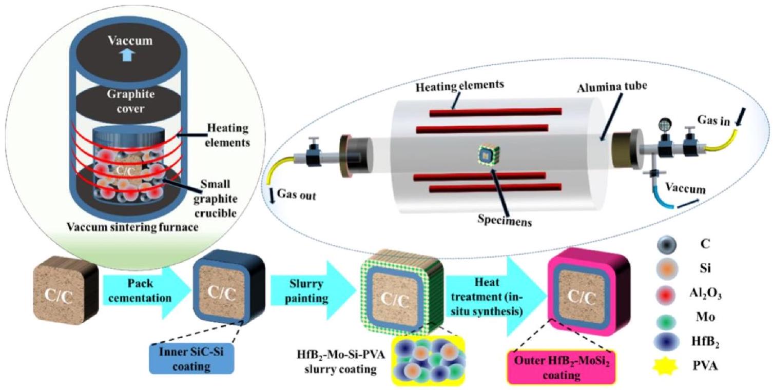
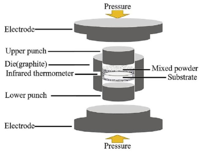
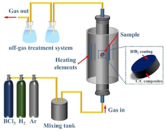
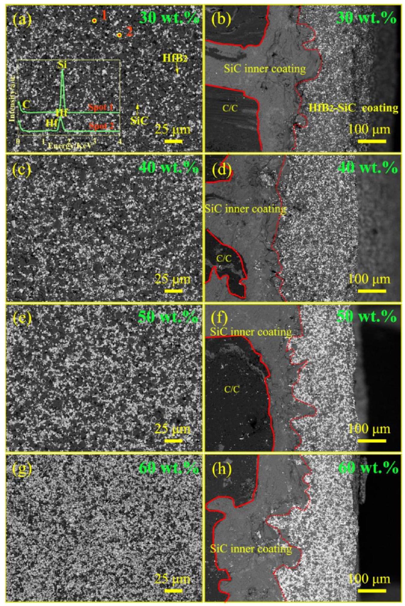
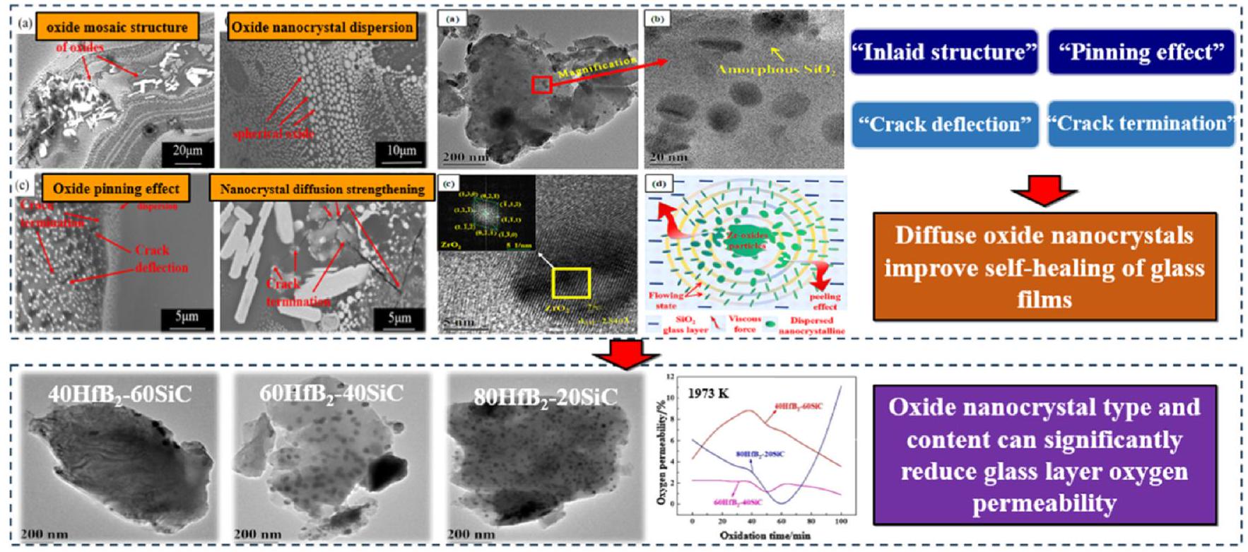
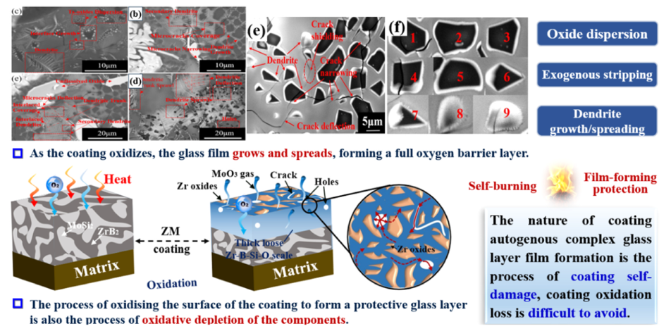
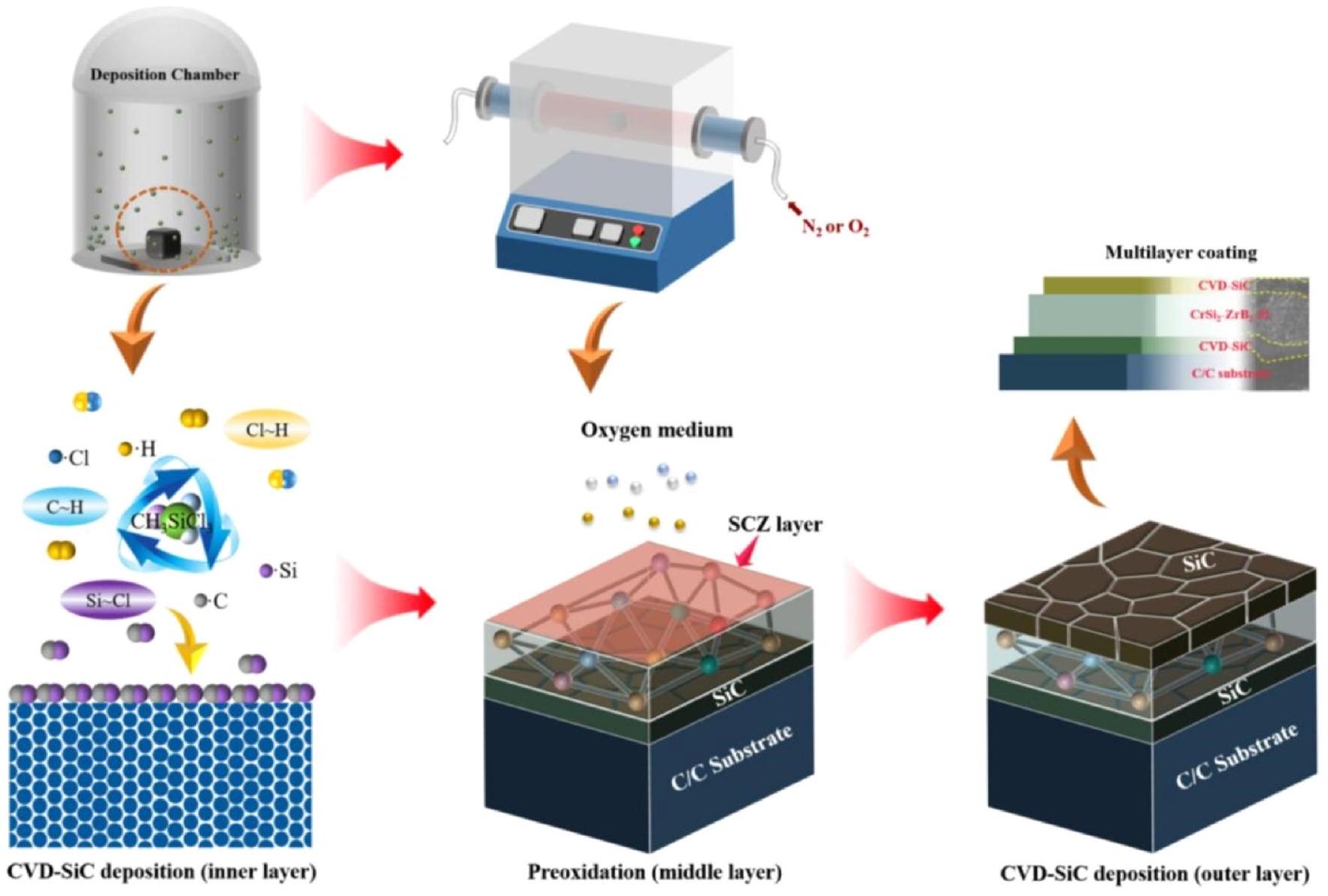
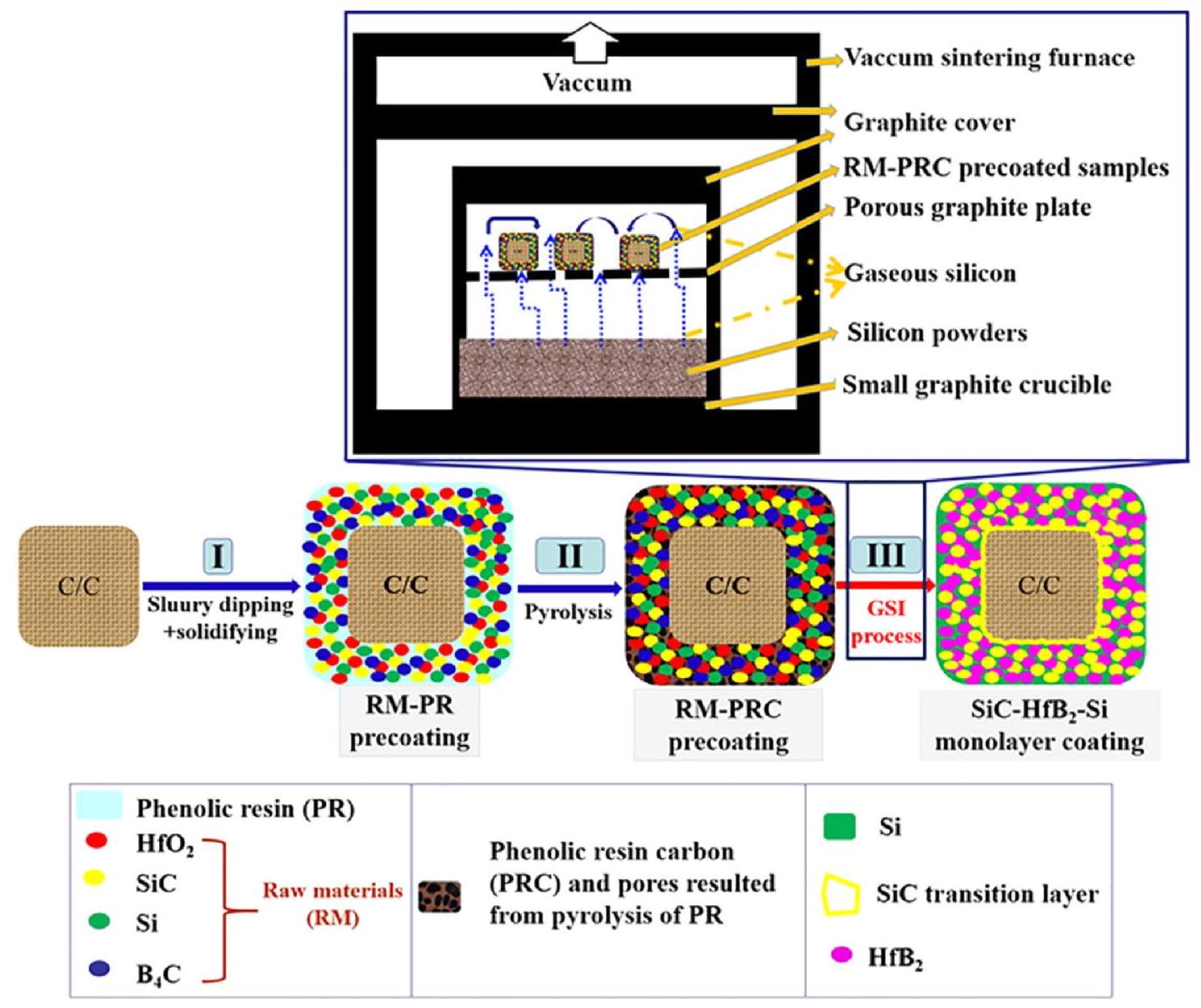
| Coating materials | Fabrication methods | Temperature ( ∘C ) | Time (h) | Mass loss (wt%) | Refs. |
|---|---|---|---|---|---|
| HfB2-SiC/SiC | PCP | 1700 | 0.8 | 0.51 g/cm2 | [115] |
| HfB2-SiC-MoSi2 | LPS | 1500 | 200 | 0.08% | [121] |
| SiO2-MexOy | CP+HT | 1700 | 30 | - | [122] |
| ZrB2-SiC-ZrC-B4C | IMP + PYR | 1500 | 200 | 1.8% | [123] |
| ZrB2-SiC-ZrC | - | 1500 | 6 | 1.34 % | [124] |
| ZrB2-SiC-TaSi2 | SCC | 1700 | 0.5 | 3.81mg/cm2 | [126] |
| ZrB2-SiC-WB | LPPS | 1500 | 753 | 0.487 % | [127] |
| HfB2-SiC-MoSi2 | LFT | 1700 | - | 0.56 % | [128] |
| SiC/SiC-MoSi2-ZrB2 | 1500 | 30 | 0.3 % | [129] | |
| ZrB2-MoSi2-SiC-Si | SI+ VSI | 1600 | 150 | 0.21 % | [130] |
| ZrB2-xMoSi2-Y2O3-yAl | SCC | 1400 | 6.5 | [133] | |
| CeO2-HfB2-MoSi2-SiC | SPS | 1700 | 1.5 | 0.14 g/cm2 | [134] |
| ZrB2-SiC-La2O3/SiC | SPS | 1800 | 0.25 | 1.15mg/cm2 | [135] |
| Lu2O3-SiC-HfB2 | SPS | 1700 | 130 | 3.8mg/cm2 | [136] |
| LaB6-HfB2-SiC | LFT | 1700 | 1.5 | 0.85 g/cm2 | [137] |
Fig. 3. (a) Backscattering cross-section micrographs of coated C/C composites; High-magnification backscattered electron micrograph of the (b) coating and (c) interface between the C/C composite and the internal SiC layer; (d) Energy dispersive spectroscopy elemental line analysis of the coating in (a), with the yellow arrow representing the scanning direction. Reproduced with permission from Ref. [
Fig. 9. Vertical crack development behavior under different conditions calculated by the smart crack growth modules of ANSYS: (a) the vertical crack development model; (b) the vertical development behavior in MoSi2 under the action of thermal stress; (c) the crack deflection behavior with weak interface; (d) the crack steering induced by micropore distribution. Reproduced with permission from Ref. [
Fig. 16. Microstructure SEM images of HfB2-SiC coatings with different HfB2 contents: (a) and (b) Surface and cross-section of the 30wt\%HfB2-SiC coating; (c) and (d) Surface and cross-section of the 40wt\%HfB2-SiC coating; (e) and (f) Surface and cross-section of the 50wt\%HfB2-SiC coating; (g) and (h) Surface and crosssection of the 60wt\%HfB2-SiC coating. Reproduced with permission from Ref. [
Fig. 19. Surface, cross-sectional morphology, and corresponding EDS analysis of ZS and ZSL coating samples after 550 h of oxidation at 1500∘C : (a) and (b) Secondary electron images of the surface of the ZS coating sample; (c) Backscattered electron image of the cross-section of the ZS coating sample; (d) and (e) Secondary electron images of the surface of the ZSL coating sample; (f) Backscattered electron image of the cross-section of the ZSL coating sample; (g) EDS area scan images of different elements corresponding to the cross-sectional morphology of the ZSL coating. Reproduced with permission from Ref. [
Fig. 34. Thickness measurements of thermally grown oxide (TGO) layers on three Si specimens after water vapor corrosion at 1300∘C : (a) APS-deposited Si coating; (b) polycrystalline Si; (c) single-crystal Si; (d) thickness comparison between unoxidized and oxidized crystalline Si. Reproduced with permission from Ref. [
Fig. 37. Experimental and simulation results under thermal shock environment: (a) mass change curves of the coated samples with monolayer MoSi 2 coating and with laminated MoSi2/Cr coating after 30 thermal cycles; (b) BSE image of monolayer MoSi2 coating (inset of figure is the surface view of (b)) and (c) BSE image of laminated MoSi2/Cr coating along the cross-section (inset of figure is the surface view of (c)) after thermal shock test; (d) and (e) stress distribution diagram along the cross-section of monolayer MoSi2 coating and laminated MoSi2/Cr coating during a thermal cycle; (f) stress distribution curves through the thickness of the coating and substrate under thermal shock environment. Reproduced with permission from Ref. [